- 您现在的位置:买卖IC网 > Sheet目录323 > DSP56311EVM (Freescale Semiconductor)KIT EVALUATION FOR DSP56311
�� �
�
�GPIO� Signals� and� Registers�
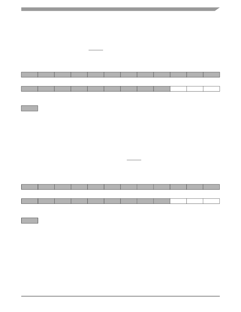
�8.7.2� Port� E� Direction� Register� (PRRE)�
�The� read/write� PRRE� controls� the� direction� of� SCI� GPIO� signals.� When� port� signal[i]� is�
�configured� as� GPIO,� PRRE[i]� controls� the� port� signal� direction.� When� PRRE[i]� is� set,� the� GPIO�
�port� signal[i]� is� configured� as� output.� When� PRRE[i]� is� cleared,� the� GPIO� port� signal[i]� is�
�configured� as� input.� A� hardware� RESET� signal� or� a� software� RESET� instruction� clears� all� PRRE�
�bits.�
�23�
�11�
�22�
�10�
�21�
�9�
�20�
�8�
�19�
�7�
�18�
�6�
�17�
�5�
�16�
�4�
�15�
�3�
�14�
�2�
�13�
�1�
�12�
�0�
�PRRE2�
�PRRE1�
�PRRE0�
�Note:�
�For� bits� 2–0,� a� 0� configures� PEn� as� a� GPI� and� a� 1� configures� PEn� as� a� GPO.� For� the� SCI,� the� GPIO� signals� are�
�PE[2–0].� The� corresponding� direction� bits� for� Port� E� GPIOs� are� PRRE[2–0].�
�=� Reserved.� Read� as� zero.� Write� with� zero� for� future� compatibility.�
�Figure� 8-9.� Port� E� Direction� Register� (PRRE� X:$FFFF9E)�
�8.7.3� Port� E� Data� Register� (PDRE)�
�Bits� 2–0� of� the� read/write� 24-bit� PDRE� writes� data� to� or� reads� data� from� the� associated� SCI� signal�
�lines� when� configured� as� GPIO� signals.� If� a� port� signal� PE[i]� is� configured� as� an� input� (GPI),� the�
�corresponding� PDRE[i]� bit� reflects� the� value� present� on� the� input� signal� line.� If� a� port� signal� PE[i]�
�is� configured� as� an� output� (GPO),� a� value� written� to� the� corresponding� PDRE[i]� bit� is� reflected� as�
�a� value� on� the� output� signal� line.� Either� a� hardware� RESET� signal� or� a� software� RESET�
�instruction� clears� all� PDR� bits.�
�23�
�11�
�22�
�10�
�21�
�9�
�20�
�8�
�19�
�7�
�18�
�6�
�17�
�5�
�16�
�4�
�15�
�3�
�14�
�2�
�13�
�1�
�12�
�0�
�PDRE2�
�PDRE1�
�PDRE0�
�Note:�
�For� bits� 2–0,� the� value� represents� the� level� that� is� written� to� or� read� from� the� associated� signal� line� if� enabled� as� a�
�GPIO� signal� by� the� PCRE� bits.� For� SCI,� the� GPIO� signals� are� PE[2–0].� The� corresponding� data� bits� are� PDRE[2–0].�
�=� Reserved.� Read� as� zero.� Write� with� zero� for� future� compatibility.�
�Figure� 8-10.� Port� Data� Registers� (PDRE� X:$FFFF9D)�
�DSP56311� User’s� Manual,� Rev.� 2�
�Freescale� Semiconductor�
�8-23�
�发布紧急采购,3分钟左右您将得到回复。
相关PDF资料
DSPAUDIOEVMMB1E
BOARD MOTHER DSP563XX
DSPIC30F2010 DEVELOPMENT KIT
KIT DEV EMBEDDED C
DSTRM-KT-0181A
DSTREAM DEBUG AND TRACE UNIT
DSUT1CSU
SURGE SUPPR NETWORK W/GROUND
DTEL2
SURGE SUPPRESSOR PHONE RJ11/RJ45
DV003001
PROGRAMMER PICSTART PLUS 16C/17C
DV164035
MPLAB ICD3 IN-CIRC DEBUGGER
DV164039
KIT DEV PIC24FJ256DA210
相关代理商/技术参数
DSP56311EVMIG_D
制造商:未知厂家 制造商全称:未知厂家 功能描述:DSP56311EVMIG DSP56311EVM Sample Code
DSP56311EVMUM
制造商:未知厂家 制造商全称:未知厂家 功能描述:DSP56311 Evaluation Module Hardware Reference Manual
DSP56311FACT
制造商:未知厂家 制造商全称:未知厂家 功能描述:DSP56311 Higher performance programmable DSP for demanding voice and data applications
DSP56311UM
制造商:未知厂家 制造商全称:未知厂家 功能描述:DSP56311 24-Bit Digital Signal Processor Users Manual
DSP56311UMAD
制造商:未知厂家 制造商全称:未知厂家 功能描述:DSP56311 Users Manual Addendum
DSP56311VF150
功能描述:数字信号处理器和控制器 - DSP, DSC 150Mhz/300MMACS 150Mhz EFCOP RoHS:否 制造商:Microchip Technology 核心:dsPIC 数据总线宽度:16 bit 程序存储器大小:16 KB 数据 RAM 大小:2 KB 最大时钟频率:40 MHz 可编程输入/输出端数量:35 定时器数量:3 设备每秒兆指令数:50 MIPs 工作电源电压:3.3 V 最大工作温度:+ 85 C 封装 / 箱体:TQFP-44 安装风格:SMD/SMT
DSP56311VF150B1
功能描述:数字信号处理器和控制器 - DSP, DSC 24 BIT DSP
RoHS:否 制造商:Microchip Technology 核心:dsPIC 数据总线宽度:16 bit 程序存储器大小:16 KB 数据 RAM 大小:2 KB 最大时钟频率:40 MHz 可编程输入/输出端数量:35 定时器数量:3 设备每秒兆指令数:50 MIPs 工作电源电压:3.3 V 最大工作温度:+ 85 C 封装 / 箱体:TQFP-44 安装风格:SMD/SMT
DSP56311VF150R2
功能描述:数字信号处理器和控制器 - DSP, DSC 24 BIT DSP RoHS:否 制造商:Microchip Technology 核心:dsPIC 数据总线宽度:16 bit 程序存储器大小:16 KB 数据 RAM 大小:2 KB 最大时钟频率:40 MHz 可编程输入/输出端数量:35 定时器数量:3 设备每秒兆指令数:50 MIPs 工作电源电压:3.3 V 最大工作温度:+ 85 C 封装 / 箱体:TQFP-44 安装风格:SMD/SMT